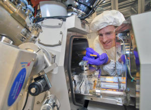
Kim Kisslinger, seen here with a focused-ion beam instrument, reduced the InGaN samples to a thickness of just 20 nanometers to prepare them for electron microscopy.
From the high-resolution glow of flat screen televisions to light bulbs that last for years, light-emitting diodes (LEDs) continue to transform technology. The celebrated efficiency and versatility of LEDs -- and other solid-state technologies including laser diodes and solar photovoltaics -- make them increasingly popular. Their full potential, however, remains untapped, in part because the semiconductor alloys that make these devices work continue to puzzle scientists.
A contentious controversy surrounds the high intensity of one leading LED semiconductor -- indium gallium nitride (InGaN) -- with experts split on whether or not indium-rich clusters within the material provide the LED's remarkable efficiency. Now, researchers from the Massachusetts Institute of Technology (MIT) and the U.S. Department of Energy's (DOE) Brookhaven National Laboratory have demonstrated definitively that clustering is not the source. The results -- published online May 16 in Applied Physics Letters -- advance fundamental understanding of LED technology and open new research pathways.
"This discovery helps solve a significant mystery in the field of LED research and demonstrates breakthrough experimental techniques that can advance other sensitive and cutting-edge electronics," said Silvija Gradečak, the Thomas Lord Associate Professor of Materials Science and Engineering at MIT and a coauthor on the study. "The work brings us closer to truly mastering solid-state technologies that could supply light and energy with unprecedented efficiency."
Building a Better Bulb
Incandescent lights -- the classic bulbs that use glowing wires of tungsten or other metals -- convert only about five percent of their energy into visible light, with the rest lost as heat. Fluorescent lights push that efficiency up to about 20 percent, still wasting 80 percent of the electricity needed to keep homes and businesses bright. In both of these instances, light is only the byproduct of heat-generating reactions rather than the principal effect, making the technology inherently inefficient.
"Solid-state lights convert electric current directly into photons," said Eric Stach, leader of the Electron Microscopy Group at Brookhaven Lab's Center for Functional Nanomaterials (CFN) and a co-author on the study. "LED bulbs use semiconductors to generate light in a process called electroluminescence. The efficiency of this process could, in theory, be nearly perfect, but the experimental realization has not reached those levels. That disconnect helped motivate this study."
For this study, the scientists looked at the LED compound InGaN (pronounced in-gan), which is particularly promising for practical applications. InGaN alloys contain dislocations -- structural imperfections that could inhibit electricity flow and light production -- but somehow the alloy performs exceptionally well. To understand the light-emitting reactions, physicists needed to understand what was happening on the atomic scale. After researchers started to investigate, however, not everyone reached the same conclusions.
Controversial Clusters
"Years ago, a team of researchers used electron microscopes to examine InGaN samples, and they identified a surprising phenomenon -- the material appeared to be spontaneously decomposing and forming these isolated indium-rich clusters," Stach said. "This behavior could explain the efficient light emission, as the clusters might help electrons avoid the structural problems in the InGaN. But then things became really interesting when another group proposed that the electron microscope itself caused that clustering decomposition. We had a real divide in the semiconductor field."
Rather than using light to examine materials, electron microscopes bombard samples with finely tuned beams of electrons and detect their interactions when they pass through a sample to reveal atomic structures. To achieve high enough resolution to examine the InGaN alloys, the electron microscopes used in the older experiments needed high-voltage beams. The controversy revolved around whether or not the experiment itself produced the clusters, rather than discovering the mechanism behind efficient light emission.
Improved Imaging
"The state-of-the-art instruments available at Brookhaven Lab's CFN changed the way we could test these promising materials," Gradečak said. "The CFN's aberration-corrected scanning transmission electron microscope (STEM) opened a new and non-destructive window into the LED samples. For the first time, we could get Ångstrom-level details -- that's one tenth of one nanometer -- without the risk of the device affecting the sample."
The researchers combined the leading STEM techniques with high-resolution electron energy loss spectroscopy (EELS), which measured the energy lost by electrons as they passed through the sample. Post-doctoral researchers Kamal Baloch of MIT -- the lead author of the study -- and Aaron Johnston-Peck of CFN actually applied these imaging techniques to the same samples that first launched the controversy over clustering, helping further settle the issue.
"We found that the indium-rich clusters do not actually exist in these samples, even though they remain efficient light emitters," Baloch said. "While clustering may still occur in other samples, which may be prepared in different ways, the important point is that we've established a foolproof method for investigating InGaN materials. We can use these non-destructive imaging techniques to explore the fundamental relationship between cluster formation and light emission to help unlock the secrets of this amazing alloy."
Beyond the advanced imaging instruments, researchers used the expertise of Brookhaven Lab physicist Kim Kisslinger, who specializes in nanoscale sample preparation. The InGaN samples were reduced to a thickness of just 20 nanometers, an essential step in priming the materials for STEM and EELS experimentation. The samples were also painstakingly cleaned and polished to eliminate artifacts that might impact image resolution.
The research was supported by the Center for Excitonics, an Energy Frontier Research Center funded by the U.S. Department of Energy's Office of Science. The work at Brookhaven Lab's Center for Functional Nanomaterials was also supported by DOE's Office of Science, with additional work carried out at the MIT Center for Materials Science Engineering.

